PCB Grounding Techniques Explained: Planes and Returns
PCB grounding is the way a printed circuit board gives every circuit a common voltage reference and a low impedance path for return current. Good grounding uses a solid ground plane next to the signal layer, short connections to it, separated return paths for noisy and sensitive circuits, and no slots under fast signals.
PCB grounding is about where current goes after it has done its work. Every current that leaves a driver comes back to its source, and on most boards it comes back through ground. If that path is long, narrow or shared with other circuits, the returning current develops a voltage across it, and that voltage shows up as noise, ground bounce or radiated emissions.
What ground does on a PCB
Ground does two separate jobs on a board:
- It is the reference that every voltage is measured against. An ADC compares its input with its own ground pin, and a logic gate decides high or low against its ground pin.
- It is the return path for current. Current flows in loops, so the ground copper carries the same current as the signal or supply trace, in the opposite direction.
Copper is not a perfect conductor. Any ground path has resistance and inductance, so return current creates a voltage drop:
At DC and low frequency the I R term dominates. With fast edges, the L di/dt term takes over, and it is the source of ground bounce in digital circuits (Johnson and Graham). Two points that are both labelled GND on the schematic can therefore sit at different voltages on the real board.
Where return current flows
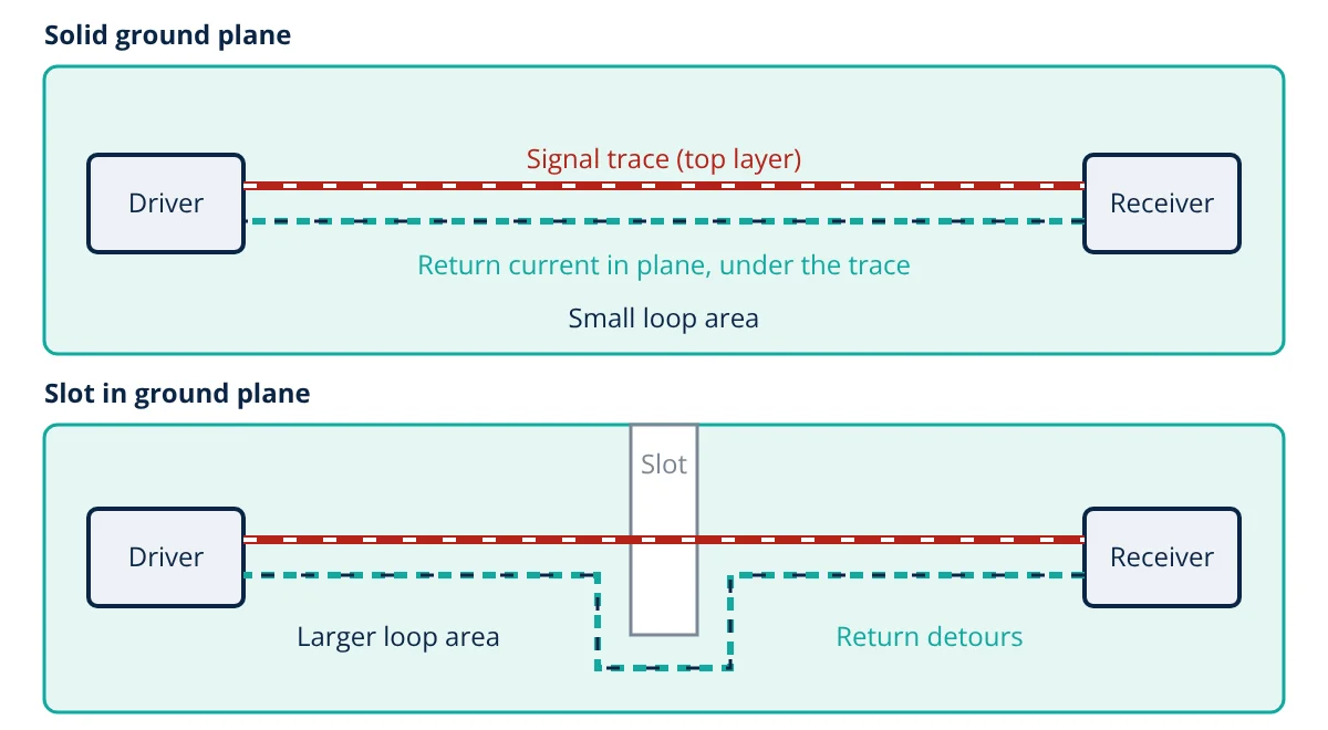
Return current takes the path of lowest impedance. Ott explains that at low frequency this is the path of least resistance, so the current spreads out across a plane. At high frequency inductance dominates, and the path of least inductance is the one that keeps the loop area smallest. On a board with a ground plane, that is the strip of plane directly beneath the signal trace.
A solid plane lets every signal set up its own return path right under itself, with no routing effort from the designer. Cutting the plane takes that away. A slot, a row of closely spaced via antipads or a split between two planes makes the return current go around, and the loop grows (Bogatin; Montrose).
Loop area matters because a current loop behaves like a small antenna. For a small loop, Ott gives the radiated electric field as:
The field rises with the square of frequency and in direct proportion to loop area, so halving the loop area halves the emission.
Main PCB grounding techniques
Single-point and multipoint grounds
In a single-point (star) ground, each circuit has its own return to one common point, so return currents from different circuits do not share copper. Ott recommends single-point grounds below about 1 MHz. At higher frequencies the long individual returns have too much inductance, so a multipoint ground is used instead: each circuit connects by the shortest route to a nearby ground plane. Ott places multipoint grounding above about 10 MHz, with hybrid schemes between the two.
Solid ground planes and stack-up
A full copper ground layer gives the lowest inductance return path available on a board. On a four-layer board a common stack-up is signal, ground, power, signal, so each outer signal layer sits next to a plane. Keep the plane continuous under fast traces, and when a signal changes layers, place a ground via close to the signal via so the return current can change reference layers too.
Ground pours and via stitching
On two-layer boards, a copper pour connected to ground is better than thin ground traces, but traces cut it into pieces. Stitch the pour on both sides together with vias so the pieces act as one conductor. Remove isolated islands of copper that connect to nothing. For practical rules on pour clearance and stitching, see this guide to PCB copper pour.
Decoupling capacitor grounding
A decoupling capacitor supplies the fast current pulses an IC draws when it switches. Its benefit depends on the inductance of its connection, so place it next to the power pin and connect its ground pad straight to the plane through a short via. A long thin trace to ground adds inductance and defeats the capacitor. The CMOS inverter is a good example of a circuit that draws a current spike at every switching edge.
Mixed-signal boards
Data converters cause the most confusion. Analog Devices tutorial MT-031 recommends, for most boards, a single solid ground plane with the analog and digital circuits placed in separate regions, and the converter’s AGND and DGND pins both connected to the analog ground plane close to the chip. The partitioning is done by component placement, not by cutting copper. Keep fast digital traces out of the analog area so their return currents stay out of it too. The sampling theorem and anti-alias filtering only work as designed when the ground under the converter is quiet.
Chassis and safety ground
Circuit ground (0 V) is not the same as chassis or protective earth. Cables leaving the box are a major path for emissions, so filtered I/O connectors are usually bonded to chassis at the point where the cable enters. Protective earthing for mains equipment follows safety rules, covered in electrical earthing.
Worked example of a ground drop
- Given
- A motor driver returns 2 A through a ground trace 50 mm long and 1 mm wide in 1 oz copper (35 µm). A 12-bit ADC with a 3.3 V reference uses the same trace as its ground. Copper resistivity 1.72 × 10⁻⁸ Ω·m.
- Find
- The DC voltage drop along the shared trace and its size in ADC codes.
- Assumptions
- DC current only; trace at room temperature; ADC ground reference taken at the far end of the trace.
- Solution
- R = ρL ÷ (W t) = 1.72 × 10⁻⁸ × 0.05 ÷ (0.001 × 35 × 10⁻⁶) = 0.0246 Ω
V = I R = 2 × 0.0246 = 0.049 V = 49 mV
1 LSB = 3.3 V ÷ 4096 = 0.806 mV
Error = 49 ÷ 0.806 = 61 LSB - Answer
- About 49 mV of ground shift, roughly 61 LSB of error on the ADC reading
- Limitations
- Real motor current also has fast edges, so the L di/dt drop adds to this figure. The fix is to give the motor its own return path to the supply and keep that current out of the ADC ground, not just to widen the trace.
Key formulas for PCB grounding
| Quantity | Formula | Symbols and units |
|---|---|---|
| Ground voltage drop | V = I R + L di/dt | I in A, R in Ω, L in H, di/dt in A/s |
| Trace or plane resistance | R = ρL ÷ (W t) | ρ = 1.72 × 10⁻⁸ Ω·m for copper, L, W, t in m |
| Sheet resistance of copper | R_s = ρ ÷ t | about 0.49 mΩ per square for 35 µm copper |
| ADC step size | LSB = V_ref ÷ 2ⁿ | n = number of bits |
| Loop radiated field (Ott) | E = 263 × 10⁻¹⁶ f² A I ÷ r | E in V/m, f in Hz, A in m², I in A, r in m |
Common PCB grounding mistakes
- Routing a fast signal across a gap between two planes.
- Sharing one ground trace between a high-current load and a precision sensor.
- Connecting decoupling capacitors to ground through long traces.
- Splitting the plane under a converter and then routing digital lines across the split.
- Leaving a cable shield or I/O ground with no low impedance bond to chassis.
PCB grounding interview and viva questions
- Why does high-frequency return current flow under the signal trace? At high frequency inductance dominates the impedance, and the path directly under the trace gives the smallest loop and so the lowest inductance.
- What is ground bounce? It is the voltage that appears on a ground connection when fast-changing current flows through its inductance, given by L di/dt, which shifts the reference seen by logic gates.
- When is single-point grounding preferred? At low frequency, below about 1 MHz according to Ott, where resistance dominates and keeping return currents separate matters more than inductance.
- How should the AGND and DGND pins of an ADC be connected? For most boards both go to the analog ground plane close to the chip, with one solid plane partitioned by component placement (Analog Devices MT-031).
- Why should a ground via sit next to a signal via? It lets the return current change reference planes along with the signal, keeping the loop small.
Related reading
Frequently asked questions
Should I split the ground plane between analog and digital sections?
Usually not. Analog Devices and Ott both recommend one solid ground plane for most mixed-signal boards, with the analog and digital parts placed in separate areas so their return currents do not share copper. A split plane helps only when no trace crosses the gap.
Why does a slot in the ground plane cause noise?
High-frequency return current flows in the plane directly under its signal trace. A slot forces that current to detour around the ends, which enlarges the current loop. A bigger loop has more inductance, radiates more and couples more noise into nearby circuits.
Is a ground pour on a two-layer board as good as a ground plane?
No. A pour broken up by traces gives return currents a longer and less predictable path. It is better than thin ground traces, but a four-layer board with an unbroken ground layer next to the signal layer performs much better for EMC.
References
- H. W. Ott, Electromagnetic Compatibility Engineering, Wiley, 2009
- H. W. Johnson and M. Graham, High-Speed Digital Design: A Handbook of Black Magic, Prentice Hall, 1993
- E. Bogatin, Signal and Power Integrity Simplified, 3rd ed., Prentice Hall, 2018
- M. I. Montrose, Printed Circuit Board Design Techniques for EMC Compliance, 2nd ed., Wiley-IEEE Press, 2000
- Analog Devices, MT-031 Tutorial: Grounding Data Converters and Solving the Mystery of AGND and DGND
- IPC-2221, Generic Standard on Printed Board Design
Get one engineering email a week
New articles, worked examples and study notes every week. Free, no spam, unsubscribe any time.

Electronics and Telecommunication engineer working in industrial instrumentation and automation. Writes the Electronics Engineering articles on Zenta Engineering. Editorial policy.