PCB Design Basics: Layers, Traces and Design Rules
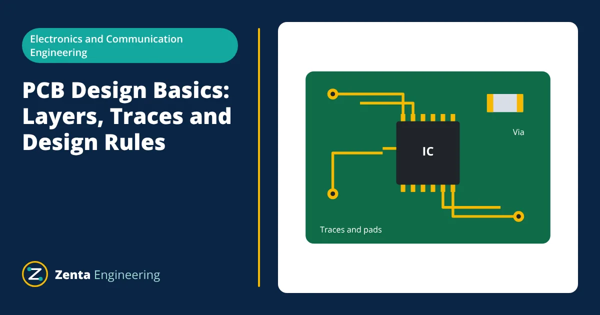
A printed circuit board (PCB) holds and connects electronic components using copper tracks on an insulating board. Good PCB design means choosing the right layer stack, sizing traces for their current, keeping enough clearance for the voltage, placing components so that high-current and high-speed loops are short, and following the design rules of the board manufacturer.
How a PCB is built
A standard rigid PCB is a sandwich of materials:
| Layer | Material | Purpose |
|---|---|---|
| Substrate (core and prepreg) | Glass-reinforced epoxy, most often FR-4 | Mechanical support and electrical insulation |
| Copper | Copper foil, commonly 1 oz/ft² (about 35 µm) | Traces, pads and planes |
| Solder mask | Coloured polymer coating, often green | Insulates copper and stops solder bridging |
| Silkscreen | Printed ink | Component outlines, labels and reference designators |
| Surface finish | HASL, ENIG, OSP or similar | Protects exposed pads and helps soldering |
A common finished thickness is 1.6 mm. Boards are described by their number of copper layers: single-sided, double-sided, or multilayer with four, six or more layers bonded together.
Key PCB features
- Traces (tracks): copper paths that connect pads.
- Pads: copper areas where component leads or terminals are soldered. Through-hole pads have a plated hole; surface mount pads sit on the surface.
- Vias: plated holes that connect layers. Through vias pass through the whole board; blind vias connect an outer layer to an inner one; buried vias connect inner layers only.
- Planes: large copper areas, usually ground or power, that give low impedance supply paths and a clean return path for signals.
- Thermal reliefs: spoke connections between a pad and a plane, which make soldering easier by limiting heat flow into the plane.
The PCB design workflow
- Schematic capture. Draw the circuit, assign component values and part numbers.
- Footprints. Link each part to a land pattern that matches its package dimensions.
- Board outline and stack-up. Define the shape, mounting holes, layer count and layer order.
- Placement. Position components, starting with connectors and mechanically fixed parts, then critical circuits such as power supplies, clocks and analog front ends.
- Routing. Draw traces and planes, following width, clearance and impedance rules.
- Design rule check (DRC). Let the software check spacing, widths, unconnected nets and drill sizes against the manufacturer’s capabilities.
- Output files. Generate Gerber or ODB++ files, drill files, a bill of materials and pick-and-place data.
Trace width and current
A trace heats up as current flows through its resistance. Its width must keep the temperature rise acceptable. IPC-2221 gives a widely used empirical relationship:
Here I is the current in amperes, ΔT the temperature rise in °C, A the cross-sectional area in square mils, and k is 0.048 for outer layers and 0.024 for inner layers. The trace width is the area divided by the copper thickness. IPC-2152 is the newer standard based on more detailed testing and often allows narrower traces, especially where planes help spread heat.
- Given
- 2 A continuous current on an outer layer, 1 oz copper (1.38 mil thick), allowed temperature rise 10 °C.
- Find
- Minimum trace width using IPC-2221.
- Assumptions
- Single isolated trace in still air; IPC-2221 outer layer constant k = 0.048.
- Solution
- 10^0.44 = 2.75, so k × ΔT^0.44 = 0.048 × 2.75 = 0.132
A = (2 / 0.132)^(1 / 0.725) = 15.1^1.379 = 42 mil²
Width = 42 / 1.38 = 30.5 mil - Answer
- About 31 mil, or 0.78 mm; round up to at least 0.8 mm
- Limitations
- The formula is conservative for many layouts and does not account for nearby planes, board thickness or multiple parallel traces. Also check the voltage drop along long traces.
Clearance and creepage
Conductors at different voltages need enough spacing to prevent arcing and leakage. IPC-2221 gives minimum electrical clearances that increase with voltage and depend on whether the conductors are internal, coated or bare on the surface. For mains-powered products, safety standards such as IEC 62368-1 set creepage (distance along the surface) and clearance (distance through air) between hazardous and safe circuits, and these are usually much larger than the PCB fabrication minimums.
Layout good practice
- Use a solid ground plane on at least one layer. It gives every signal a short return path directly under its trace, which reduces noise and radiated emissions.
- Place decoupling capacitors close to IC power pins, with short connections to the pin and to ground, so they can supply fast current pulses.
- Keep switching power loops small. In a buck converter, the input capacitor, switch and diode or low-side MOSFET form a loop carrying fast-changing current; it should be as compact as possible.
- Separate noisy and sensitive circuits by placement, keeping analog inputs away from switching nodes and clock lines.
- Control impedance for high-speed signals such as USB, Ethernet and DDR memory, using the stack-up and trace widths the manufacturer specifies.
- Avoid splitting planes under fast signals, because a gap in the return path forces current to detour and radiate.
- Think about heat: add copper area and thermal vias under hot components such as regulators and power MOSFETs.
Design for manufacture
Every fabricator publishes minimum trace width and spacing, drill sizes, annular ring and solder mask limits. Designing well inside those limits improves yield and lowers cost. Typical good practice includes adding fiducial marks for automated assembly, keeping components away from the board edge, giving test points to key signals and making silkscreen labels readable after assembly.
Common mistakes to avoid
- Using a footprint that does not match the exact package of the purchased part.
- Placing decoupling capacitors far from the IC, connected through long thin traces.
- Routing high-current paths with default thin traces.
- Leaving no test points for programming and debugging.
- Forgetting to check silkscreen orientation marks for diodes, polarised capacitors and ICs.
Applications
PCBs are used in nearly every electronic product: consumer devices, industrial controllers, power supplies, automotive modules, medical equipment and communication systems. The same design principles apply from a simple two-layer sensor board to a twelve-layer processor board, with more attention to signal integrity as speeds rise.
Related reading
Frequently asked questions
What does 1 oz copper mean on a PCB?
It means one ounce of copper spread over one square foot of board, which gives a thickness of about 35 µm (1.4 mil). Heavier copper, such as 2 oz, is used for higher currents.
How many layers does my PCB need?
Simple, low-speed circuits often fit on two layers. Four layers, with inner ground and power planes, make routing easier and greatly improve noise and EMC performance for microcontroller, high-speed or RF designs.
What is a via?
A via is a plated hole that connects copper on different layers. Through-hole vias go through the whole board; blind and buried vias connect only some layers and are used in dense designs.
References
- IPC-2221, Generic Standard on Printed Board Design
- IPC-2152, Standard for Determining Current Carrying Capacity in Printed Board Design
- IPC-A-600, Acceptability of Printed Boards
- M. I. Montrose, Printed Circuit Board Design Techniques for EMC Compliance, Wiley-IEEE Press
Get one engineering email a week
New articles, worked examples and study notes every week. Free, no spam, unsubscribe any time.

Electronics and Telecommunication engineer working in industrial instrumentation and automation. Writes the Electronics Engineering articles on Zenta Engineering. Editorial policy.