Transistor Working Principle: BJT Basics
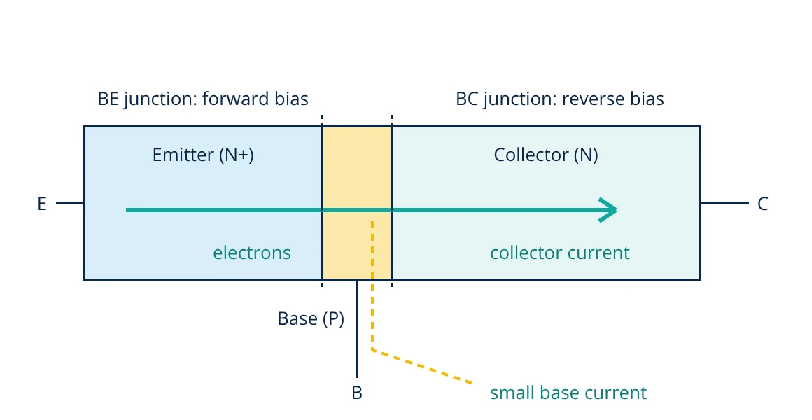
The transistor working principle of a bipolar junction transistor (BJT) is that a small current into the base controls a much larger current from collector to emitter. With the base-emitter junction forward biased and the base-collector junction reverse biased, carriers injected from the emitter cross a thin base and are swept into the collector, so IC ≈ β IB.
The transistor is the building block of amplifiers, switches, oscillators and digital logic. The bipolar junction transistor was the first type to be mass produced, and it is still widely used for discrete switching, analog amplifiers and power stages. This guide explains its structure, how it works inside, the equations that describe it, its operating regions, and how to design a simple transistor switch.
Construction of a BJT
A BJT is made of three doped semiconductor regions forming two PN junctions. In an NPN transistor a thin P-type base sits between an N-type emitter and an N-type collector. A PNP transistor has the opposite arrangement. The three regions are not alike:
- Emitter: heavily doped, so it can inject a large number of carriers into the base.
- Base: very thin and lightly doped, so most injected carriers pass through without recombining.
- Collector: moderately doped and physically the largest region, because it must collect the carriers and dissipate most of the heat.
The circuit symbol has an arrow on the emitter showing the direction of conventional current: out of the emitter for NPN, into the emitter for PNP. If you are new to PN junctions, the article what is a diode explains forward and reverse bias first.
Transistor working principle step by step
The description below is for an NPN device in the forward-active mode. For PNP the roles of electrons and holes, and all polarities, are reversed.
- Bias the junctions. The base-emitter (BE) junction is forward biased, about 0.6 to 0.7 V for silicon. The base-collector (BC) junction is reverse biased by making the collector more positive than the base.
- Emitter injects electrons. Forward bias lowers the BE barrier, and the heavily doped emitter injects a large flow of electrons into the base.
- Electrons diffuse across the base. Because the base is thin and lightly doped, few electrons find holes to recombine with. The few that do, plus holes injected from base into emitter, make up the small base current IB.
- Collector sweeps them up. Electrons reaching the edge of the reverse biased BC depletion region are pulled across by its electric field into the collector. This forms the collector current IC.
- Control. Raising VBE slightly raises the injection exponentially, so the base terminal controls the collector current while drawing only a small current itself.
BJT current equations
Kirchhoff’s current law at the device gives:
The common-emitter current gain β (also written hFE for the DC value) and the common-base gain α are:
β for small signal transistors is typically in the range of about 50 to 300, and it varies widely between devices of the same type and with temperature and collector current. Good designs therefore never depend on an exact value of β. α is slightly less than 1.
In the active region, the collector current depends exponentially on the base-emitter voltage:
where IS is the saturation current and VT is the thermal voltage, about 25.9 mV at 300 K. This exponential law is why VBE stays near 0.7 V over a wide range of currents: a tenfold change in IC changes VBE by only about 60 mV.
Operating regions
| Region | BE junction | BC junction | Behaviour | Typical use |
|---|---|---|---|---|
| Cutoff | Reverse or zero bias | Reverse bias | Almost no current flows | Switch OFF |
| Forward-active | Forward bias | Reverse bias | IC ≈ β IB | Amplifier |
| Saturation | Forward bias | Forward bias | VCE small, about 0.1 to 0.3 V | Switch ON |
| Reverse-active | Reverse bias | Forward bias | Low gain | Rarely used |
In saturation the collector current is limited by the external circuit, not by β. Logic families such as TTL use transistors switching between cutoff and saturation; the logic gates article shows the gate functions they build.
Transistor configurations
- Common emitter: input at base, output at collector. Gives both voltage and current gain with phase inversion; the most common amplifier stage.
- Common collector (emitter follower): output at emitter. Voltage gain just below 1, high input resistance, low output resistance; used as a buffer.
- Common base: input at emitter. Current gain just below 1 but good high frequency response.
Using a BJT as a switch
To switch a load such as a relay, LED string or small motor from a microcontroller pin, the transistor is driven hard into saturation. Horowitz and Hill recommend supplying more base current than the minimum IC / β, commonly designing for a ratio of collector to base current of about 10 (a “forced beta” of 10), so that the transistor stays saturated even with a low-gain device. An inductive load also needs a flyback diode across it.
- Given
- An NPN transistor switches a 30 mA load from a 12 V supply. The base is driven from a 5 V logic output. VBE = 0.7 V when ON.
- Find
- A suitable base resistor RB and the resulting forced beta.
- Assumptions
- Design for a forced beta of 10; the logic output reaches 5 V and can source a few milliamperes; the transistor’s minimum β is well above 10.
- Solution
- Required base current IB = IC / 10 = 30 / 10 = 3.0 mA
RB = (5 − 0.7) / 0.003 = 1433 Ω
The nearest E12 value is 1.5 kΩ, slightly higher, so check it:
IB = 4.3 / 1500 = 2.87 mA
Forced beta = 30 / 2.87 = 10.5 - Answer
- RB = 1.5 kΩ gives about 2.9 mA of base current and a forced beta of about 10.5, which keeps the transistor well saturated
- Limitations
- Check the logic output’s current rating and the transistor’s datasheet for VCE(sat), maximum collector current and power dissipation. VBE rises slightly at higher base current.
Advantages and limitations of the BJT
- Advantages: high transconductance for a given current, predictable VBE, low noise in many analog stages, simple to drive at low voltages.
- Limitations: needs continuous base current, which wastes power in switching; slower to turn off from saturation because stored charge must be removed; current gain varies with temperature and between devices; risk of thermal runaway in power stages without emitter resistance.
For switching at higher power and speed, MOSFETs are often preferred. The CMOS inverter article shows how MOSFETs build digital logic, and TTL vs CMOS logic families on InstrumentationBlog.in compares the two technologies.
Related reading
Frequently asked questions
Why is the base of a BJT made thin and lightly doped?
Electrons injected from the emitter must cross the base and reach the collector before they recombine with holes. A thin, lightly doped base has few holes and a short path, so only a small fraction of the carriers recombine. That small fraction is the base current, which keeps the current gain high.
Can the emitter and collector of a BJT be swapped?
The transistor will still conduct in the reverse-active mode, but with a much lower current gain. The emitter is heavily doped and the collector is larger and more lightly doped, so the two regions are not interchangeable in practice.
What is the difference between a BJT and a MOSFET?
A BJT is current controlled: a base current controls a larger collector current, and both electrons and holes take part in conduction. A MOSFET is voltage controlled: the gate voltage sets the channel conductance and almost no steady gate current flows.
References
- A. S. Sedra, K. C. Smith, T. C. Carusone and V. Gaudet, Microelectronic Circuits, 8th ed., Oxford University Press
- R. L. Boylestad and L. Nashelsky, Electronic Devices and Circuit Theory, 11th ed., Pearson
- P. Horowitz and W. Hill, The Art of Electronics, 3rd ed., Cambridge University Press
- D. A. Neamen, Semiconductor Physics and Devices: Basic Principles, 4th ed., McGraw-Hill
- S. M. Sze and K. K. Ng, Physics of Semiconductor Devices, 3rd ed., Wiley
Get one engineering email a week
New articles, worked examples and study notes every week. Free, no spam, unsubscribe any time.

Electronics and Telecommunication engineer working in industrial instrumentation and automation. Writes the Electronics Engineering articles on Zenta Engineering. Editorial policy.