Logic Gates: Types and Truth Tables Explained
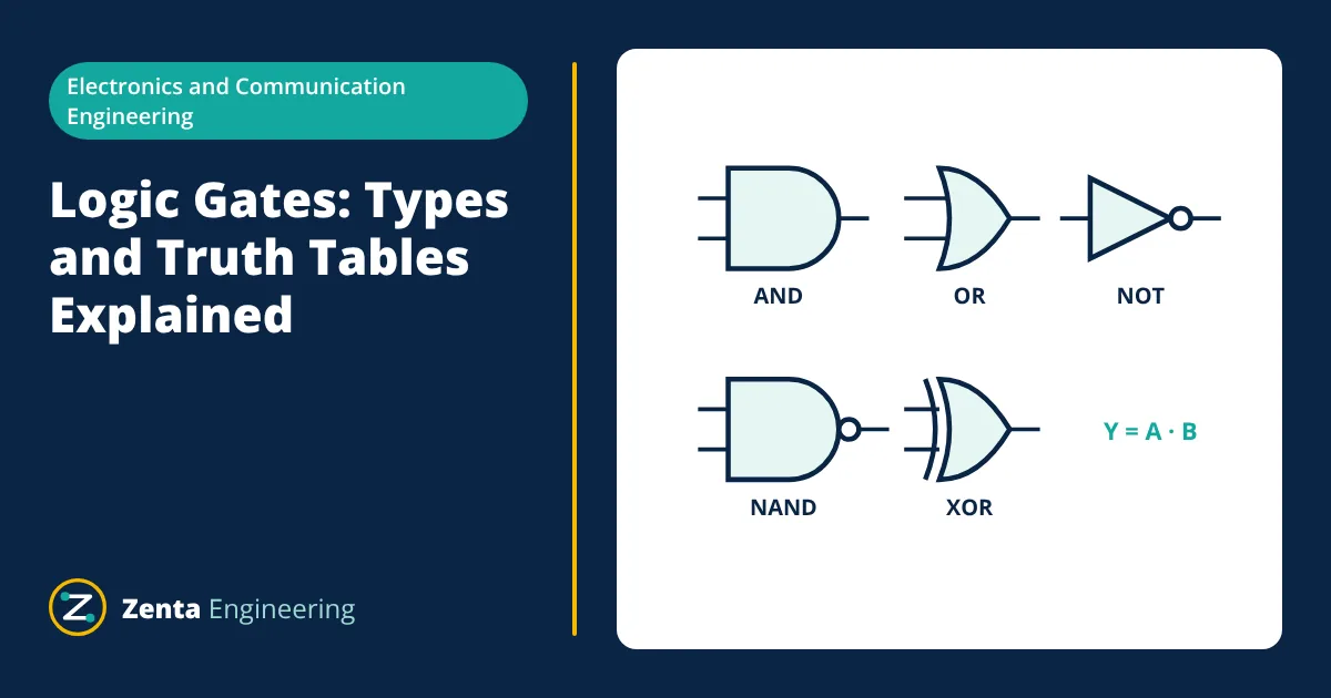
Logic gates are the building blocks of digital electronics. A logic gate is a circuit that produces a binary output (0 or 1) from one or more binary inputs according to a fixed rule. The seven basic gates are NOT, AND, OR, NAND, NOR, XOR and XNOR. Every digital system, from a simple counter to a microprocessor, is built from combinations of these gates.
Binary logic
Digital circuits represent information with two voltage levels: a high level for logic 1 (true) and a low level for logic 0 (false). A logic gate is described completely by its truth table, which lists the output for every possible combination of inputs. A gate with n inputs has 2ⁿ rows in its truth table.
The rule of a gate can also be written as a Boolean expression. In Boolean algebra, a dot or juxtaposition means AND (A·B or AB), a plus sign means OR (A + B), a bar or prime means NOT (A′), and ⊕ means XOR.
The basic gates
| Gate | Boolean expression | Output is 1 when |
|---|---|---|
| NOT (inverter) | Y = A′ | The input is 0 |
| AND | Y = A·B | All inputs are 1 |
| OR | Y = A + B | At least one input is 1 |
| NAND | Y = (A·B)′ | At least one input is 0 |
| NOR | Y = (A + B)′ | All inputs are 0 |
| XOR | Y = A ⊕ B | The inputs are different |
| XNOR | Y = (A ⊕ B)′ | The inputs are the same |
Truth table for two-input gates
| A | B | AND | OR | NAND | NOR | XOR | XNOR |
|---|---|---|---|---|---|---|---|
| 0 | 0 | 0 | 0 | 1 | 1 | 0 | 1 |
| 0 | 1 | 0 | 1 | 1 | 0 | 1 | 0 |
| 1 | 0 | 0 | 1 | 1 | 0 | 1 | 0 |
| 1 | 1 | 1 | 1 | 0 | 0 | 0 | 1 |
The NOT gate has a single input: an input of 0 gives an output of 1, and an input of 1 gives 0.
Each gate has a standard schematic symbol. The distinctive-shape symbols in IEEE 91 are the most widely recognised; IEC 60617 uses rectangular symbols with a label inside, such as & for AND and ≥1 for OR. A small circle (bubble) on an input or output indicates inversion.
Universal gates
NAND and NOR are called universal gates because each one alone can build any logic function:
- NOT from NAND: connect both inputs together, so Y = (A·A)′ = A′.
- AND from NAND: follow a NAND gate with a NAND wired as an inverter.
- OR from NAND: invert each input with a NAND, then NAND the results, because (A′·B′)′ = A + B.
- XOR from NAND: four NAND gates are enough.
The same constructions exist for NOR. In CMOS technology, NAND and NOR gates need fewer transistors than AND and OR, which is one reason they are so widely used.
De Morgan’s theorems
De Morgan’s theorems show how to swap between AND and OR forms:
- (A·B)′ = A′ + B′: a NAND equals an OR with inverted inputs.
- (A + B)′ = A′·B′: a NOR equals an AND with inverted inputs.
They are used to simplify logic expressions and to convert a circuit into all-NAND or all-NOR form.
Combining gates: the half adder
Gates are combined to perform arithmetic. A half adder adds two single bits A and B and produces a sum bit S and a carry bit C.
- Given
- Two input bits A and B.
- Find
- Logic expressions and gates for the sum S and carry C of A + B.
- Assumptions
- Binary addition without a carry input.
- Solution
- 0 + 0 = 0 carry 0; 0 + 1 = 1 carry 0; 1 + 0 = 1 carry 0; 1 + 1 = 0 carry 1
S is 1 only when the inputs differ, so S = A ⊕ B
C is 1 only when both inputs are 1, so C = A·B - Answer
- Sum = A XOR B, carry = A AND B: one XOR gate and one AND gate
- Limitations
- A half adder has no carry input. Adding multi-bit numbers needs full adders, each built from two half adders and an OR gate, chained together.
Logic levels and noise margin
Real gates accept a range of voltages as 0 or 1. For standard 5 V TTL logic, the datasheet values are:
| Parameter | Meaning | Standard TTL value |
|---|---|---|
| VIL(max) | Highest input voltage read as 0 | 0.8 V |
| VIH(min) | Lowest input voltage read as 1 | 2.0 V |
| VOL(max) | Highest output voltage for a 0 | 0.4 V |
| VOH(min) | Lowest output voltage for a 1 | 2.4 V |
The noise margin is the amount of noise a signal can pick up and still be read correctly. For standard TTL it is VOH − VIH = 0.4 V for the high level and VIL − VOL = 0.4 V for the low level. CMOS logic families have thresholds that scale with their supply voltage, and modern devices work at 3.3 V, 1.8 V and lower. Connecting families with different levels may need a level shifter.
Other important gate parameters
- Propagation delay: the time from an input change to the resulting output change. It limits how fast a circuit can operate.
- Fan-out: how many inputs one output can drive while keeping valid logic levels.
- Power consumption: CMOS gates draw very little current when static; most power is used when they switch, so it rises with frequency.
- Schmitt trigger inputs: some gates have hysteresis, so slow or noisy input signals produce clean output transitions.
Combinational and sequential logic
Circuits built only from gates, where the outputs depend only on the present inputs, are called combinational logic. Adders, decoders and multiplexers are examples. When gates are connected with feedback, they can store a state. Two cross-coupled NAND or NOR gates form an SR latch, the simplest memory element, and latches combine into flip-flops, registers and counters. Circuits whose outputs depend on both present inputs and stored state are called sequential logic, and they are the basis of every processor and state machine.
Where logic gates are used
- Arithmetic circuits: adders, subtractors and comparators inside processors.
- Multiplexers and decoders: selecting data paths and memory locations.
- Control logic: interlocks, enable signals and glue logic between chips.
- Programmable logic: FPGAs and CPLDs implement millions of gates defined in a hardware description language.
Related reading
Frequently asked questions
Why are NAND and NOR called universal gates?
Any logic function, including NOT, AND, OR and XOR, can be built using only NAND gates, or only NOR gates. This let early chip designers build complete systems from a single gate type.
What is the difference between XOR and OR?
OR gives 1 when either input or both inputs are 1. XOR (exclusive OR) gives 1 only when the inputs are different, so it outputs 0 when both inputs are 1.
What happens if a CMOS input is left unconnected?
An unconnected CMOS input floats and can drift between logic levels, causing random switching, extra current and oscillation. Unused inputs should be tied to the supply or ground, directly or through a resistor.
References
- M. M. Mano and M. D. Ciletti, Digital Design, Pearson
- T. L. Floyd, Digital Fundamentals, Pearson
- Texas Instruments, Logic Guide
Get one engineering email a week
New articles, worked examples and study notes every week. Free, no spam, unsubscribe any time.

Electronics and Telecommunication engineer working in industrial instrumentation and automation. Writes the Electronics Engineering articles on Zenta Engineering. Editorial policy.