Buck Converter Working Principle and Design Equations
A buck converter steps a DC voltage down by switching a transistor on and off at high frequency and smoothing the result with an inductor and capacitor. In continuous conduction, the output voltage is the input voltage multiplied by the duty cycle D, the fraction of each period the switch is on:
Vout = D × Vin
The circuit
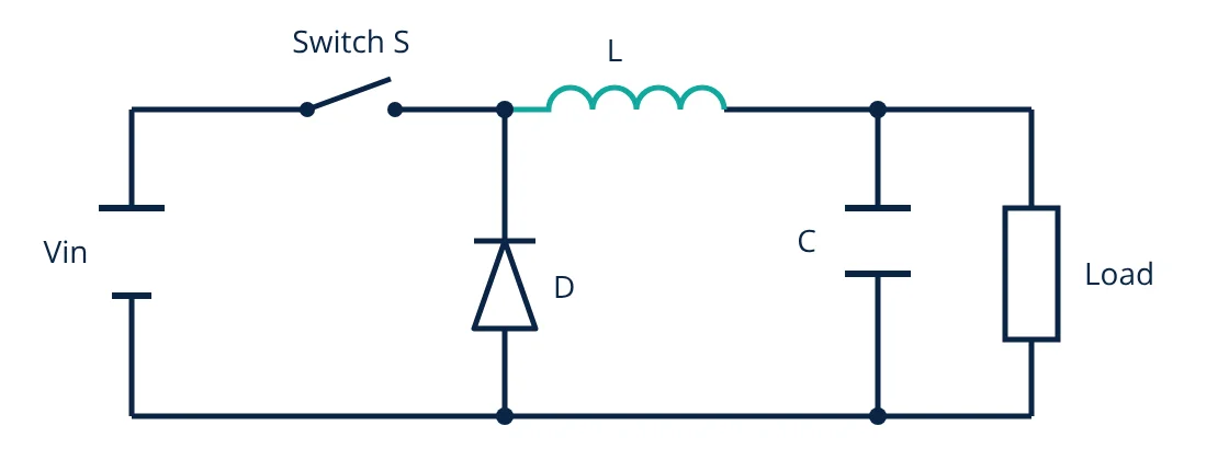
A buck converter has four power components:
- Switch S, usually a MOSFET, turned on and off by a pulse width modulation (PWM) controller.
- Diode D (or a second MOSFET in a synchronous converter), which carries the inductor current when the switch is off.
- Inductor L, which stores energy and smooths the current.
- Output capacitor C, which smooths the output voltage.
How a buck converter works
- Switch on (time D × T). The input is connected to the inductor. The voltage across the inductor is Vin − Vout, so its current rises linearly. The inductor stores energy, and current flows to the capacitor and load.
- Switch off (time (1 − D) × T). The inductor keeps its current flowing, so the switch node falls until the diode conducts. The inductor now has −Vout across it, and its current falls linearly as it releases stored energy to the load.
In steady state the inductor current must return to the same value at the end of each period. Its average voltage over a period must therefore be zero, which is called volt-second balance:
This ideal result ignores losses. In a real converter the controller adjusts D slightly upwards to make up for voltage drops in the switch, diode and inductor.
Design equations
Inductor ripple current. During the on time, the inductor current rises by:
where fsw is the switching frequency. A common starting point is to choose L so that ΔIL is about 20 to 40 percent of the maximum output current.
Peak inductor and switch current. IL(peak) = Iout + ΔIL / 2. The inductor’s saturation current rating must exceed this value with margin.
Output voltage ripple. If the capacitor’s resistance is negligible, the ripple voltage is approximately:
The capacitor’s equivalent series resistance (ESR) adds a further ripple of about ΔIL × ESR, which often dominates with electrolytic capacitors. Ceramic capacitors have very low ESR.
- Given
- Vin = 12 V, Vout = 5 V, Iout(max) = 2 A, fsw = 500 kHz, target inductor ripple 30 percent of Iout, target output ripple 10 mV.
- Find
- Duty cycle, inductor value, peak current and output capacitance.
- Assumptions
- Continuous conduction, ideal components, capacitor ESR negligible for the first estimate.
- Solution
- D = 5 / 12 = 0.417
ΔIL target = 0.3 × 2 = 0.6 A
L = 5 × (1 − 0.417) / (500,000 × 0.6) = 9.7 µH, so choose 10 µH
Actual ΔIL = 5 × 0.583 / (500,000 × 0.000010) = 0.58 A
IL(peak) = 2 + 0.58 / 2 = 2.29 A
C = 0.58 / (8 × 500,000 × 0.010) = 14.6 µF, so choose 22 µF ceramic - Answer
- D ≈ 0.42, L = 10 µH (saturation rating above 2.3 A with margin), C = 22 µF low-ESR ceramic
- Limitations
- Ceramic capacitors lose capacitance with applied DC voltage, so check the effective value at 5 V. Losses raise the real duty cycle slightly. Loop compensation must be designed for the chosen L and C.
Losses and efficiency
The main losses in a buck converter are:
- Conduction loss in the MOSFET: I² × RDS(on) during the on time.
- Switching loss: energy lost in each transition, which rises with switching frequency and input voltage.
- Diode loss: forward voltage × current during the off time. At low output voltages this is large, which is why synchronous rectification is used.
- Inductor loss: resistance of the winding (DCR) and core loss.
- Capacitor loss: ripple current flowing through ESR.
Higher switching frequency allows smaller inductors and capacitors but increases switching loss, so the frequency is a trade-off between size and efficiency.
Choosing the components
- Controller or converter IC: many designs use an integrated buck regulator that contains the MOSFETs, control loop and protection. Choose one whose input voltage range, output current and switching frequency suit the application.
- MOSFET: if discrete, select drain-source voltage rating with margin above the maximum input voltage, low RDS(on) for conduction loss, and low gate charge for switching loss.
- Diode: a Schottky diode with a reverse rating above Vin and a current rating above the output current, or a synchronous MOSFET instead.
- Inductor: inductance from the ripple calculation, saturation current above the peak current with margin, RMS current rating above the output current, and low DC resistance.
- Input capacitor: must handle a large RMS ripple current, which is close to half the output current when D is about 0.5. Low-ESR ceramic capacitors placed close to the switch are the usual choice.
- Output capacitor: sized for ripple and for load transient response, with its effective capacitance checked at the operating voltage.
Layout tips
The switching current in the input loop, made of the input capacitor, the switch and the diode or low-side MOSFET, changes very quickly. Keep this loop as small as possible, place the input capacitor right at the switch, and use a solid ground plane. Keep the feedback trace short and away from the switch node, which carries a fast square wave that can couple noise into sensitive circuits.
Continuous and discontinuous conduction
In continuous conduction mode (CCM), the inductor current never reaches zero, and Vout = D × Vin. When the load current falls below half the ripple current, the inductor current drops to zero before the end of each cycle. This discontinuous conduction mode (DCM) changes the voltage relationship, and the controller must adjust D further to hold the output.
Protection features
Practical buck regulators include protection that the basic circuit lacks: cycle-by-cycle current limiting to protect the switch and inductor, soft start to limit inrush current into the output capacitor, undervoltage lockout so the converter does not run from too low an input, and thermal shutdown.
Applications
- Point-of-load supplies that step 12 V or 5 V down to the core voltages of processors and FPGAs.
- Battery-powered devices, where efficiency directly extends run time.
- Automotive electronics, converting the vehicle battery voltage to 5 V and 3.3 V rails.
- LED drivers, where the converter regulates current instead of voltage.
Related reading
Frequently asked questions
Why is a buck converter more efficient than a linear regulator?
A linear regulator drops the excess voltage across a transistor and turns it into heat, so stepping 12 V down to 5 V wastes more than half the input power. A buck converter switches fully on and off and stores energy in an inductor, so efficiencies of 85 to 95 percent are common.
What is synchronous rectification?
It replaces the freewheeling diode with a second MOSFET that is switched on when the main switch is off. The MOSFET's low on-resistance drops much less voltage than a diode, which improves efficiency, especially at low output voltages.
What happens at very light load?
The inductor current can fall to zero during each cycle, which is called discontinuous conduction mode. The simple Vout = D × Vin relationship no longer holds, and many controllers switch to a pulse-skipping or burst mode to keep efficiency high.
References
- R. W. Erickson and D. Maksimović, Fundamentals of Power Electronics, Springer
- N. Mohan, T. M. Undeland and W. P. Robbins, Power Electronics: Converters, Applications, and Design, Wiley
- Texas Instruments, SLVA477, Basic Calculation of a Buck Converter's Power Stage
Get one engineering email a week
New articles, worked examples and study notes every week. Free, no spam, unsubscribe any time.

Electronics and Telecommunication engineer working in industrial instrumentation and automation. Writes the Electronics Engineering articles on Zenta Engineering. Editorial policy.