CMOS Inverter Working Principle
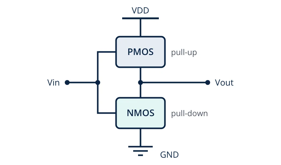
A CMOS inverter is built from one PMOS transistor connected to the supply and one NMOS transistor connected to ground, with their gates joined as the input and their drains joined as the output. When the input is low, the PMOS conducts and the output goes high; when the input is high, the NMOS conducts and the output goes low. Because one transistor is always off in steady state, the inverter draws almost no static power.
Why the inverter matters
The inverter is the simplest CMOS logic gate, and its behaviour defines how all CMOS logic works. NAND, NOR and complex gates use the same idea: a pull-up network of PMOS transistors and a complementary pull-down network of NMOS transistors. Understanding the inverter’s switching threshold, delay and power explains the speed and power limits of entire chips.
Circuit structure
- The PMOS source is connected to the supply VDD. It turns on when its gate is low relative to its source.
- The NMOS source is connected to ground. It turns on when its gate is high.
- Both gates connect to the input; both drains connect to the output, which drives the next gate’s input capacitance.
How the CMOS inverter works
| Input | PMOS | NMOS | Output |
|---|---|---|---|
| Low (0 V) | On | Off | High (VDD) |
| High (VDD) | Off | On | Low (0 V) |
With the input low, the PMOS connects the output to VDD and the NMOS is off, so the output is a strong logic 1. With the input high, the NMOS connects the output to ground and the PMOS is off, so the output is a strong logic 0. The output swings fully from rail to rail, which gives CMOS large noise margins.
Voltage transfer characteristic
Plotting Vout against Vin as the input sweeps from 0 to VDD gives the voltage transfer characteristic (VTC). It has a flat high region, a steep transition and a flat low region. Inside the transition region both transistors conduct briefly.
- The switching threshold VM is the input voltage at which Vin = Vout. For balanced transistors it is close to VDD / 2.
- VIL and VIH are the input voltages where the slope of the VTC is −1. Inputs below VIL are safely read as 0, and above VIH as 1.
- The noise margins are NML = VIL − VOL and NMH = VOH − VIH. Because VOL ≈ 0 and VOH ≈ VDD, CMOS noise margins are large.
Transistor sizing
The current a MOSFET can drive is proportional to its carrier mobility and its width-to-length ratio W/L. Electron mobility in silicon is roughly two to three times hole mobility, so an NMOS of the same size is stronger than a PMOS. To make the rise and fall times equal and place VM near VDD / 2, the PMOS is usually made about two to three times wider than the NMOS. Designers can deliberately skew the sizes to move VM or to speed up one transition.
Propagation delay
The inverter output drives a load capacitance made up of the next gates’ inputs, the wiring and its own drain capacitance. Each transition charges or discharges this capacitance through the resistance of the conducting transistor. The propagation delay is therefore roughly proportional to the product of the effective transistor resistance and the load capacitance. Larger transistors switch heavier loads faster but present more capacitance to the gate that drives them, which is the basis of buffer sizing techniques such as logical effort.
Power consumption
CMOS power has three parts:
- Dynamic switching power, from charging and discharging the load capacitance:
where α is the activity factor (the fraction of clock cycles in which the node switches), CL the load capacitance and f the clock frequency.
- Short-circuit power, during the brief time in each transition when both transistors conduct.
- Static (leakage) power, from subthreshold and gate leakage currents. It was negligible in older processes but is significant in modern nanometre processes.
- Given
- Node capacitance CL = 10 fF, VDD = 1.0 V, clock f = 1 GHz, activity factor α = 0.1.
- Find
- Dynamic power per node, and for a chip with 100 million such nodes.
- Assumptions
- All nodes identical; short-circuit and leakage power ignored.
- Solution
- P = 0.1 × 10 × 10⁻¹⁵ × 1.0² × 10⁹ = 1 × 10⁻⁶ W per node
For 10⁸ nodes: 10⁸ × 10⁻⁶ = 100 W - Answer
- 1 µW per node and about 100 W for the whole chip
- Limitations
- Real chips have widely varying node capacitances and activity. The example shows why chip designers lower VDD, gate unused clocks and reduce switching activity.
From inverter to NAND and NOR
Other CMOS gates extend the inverter’s complementary structure:
- NAND gate: two NMOS transistors in series in the pull-down network and two PMOS transistors in parallel in the pull-up network. The output goes low only when both inputs are high.
- NOR gate: two NMOS transistors in parallel in the pull-down network and two PMOS transistors in series in the pull-up network. The output goes high only when both inputs are low.
Because PMOS transistors are weaker, series PMOS stacks are slow. NAND gates, which put the series stack in the stronger NMOS network, are therefore usually preferred to NOR gates in CMOS design.
Why CMOS dominates digital design
- Very low static power, which makes high gate density possible.
- Full rail-to-rail output and large noise margins.
- High input impedance, since MOSFET gates draw no DC current.
- Scalability: shrinking transistor dimensions increases speed and density, which has driven decades of progress in processors and memory.
Supply voltage scaling
Because dynamic power depends on VDD squared, supply voltages have fallen with each process generation, from 5 V in early CMOS to around 1 V or less in modern processors. Lower voltage reduces power and allows smaller transistors, but it also reduces the current drive, slows switching and shrinks noise margins, so the threshold voltages of the transistors must be reduced too, which increases leakage.
Applications
The CMOS inverter is used as a buffer and clock driver, as a building block of ring oscillators for process monitoring, and as the basis of SRAM cells, where two cross-coupled inverters store one bit. Every CMOS logic gate in a processor, FPGA or microcontroller is an extension of the same complementary pull-up and pull-down principle.
Related reading
Frequently asked questions
Why does a CMOS inverter use almost no power when idle?
In either steady state one transistor is fully off, so there is no direct path from supply to ground. Only a tiny leakage current flows. Power is mainly used when the output switches and the load capacitance is charged and discharged.
Why is the PMOS transistor made wider than the NMOS?
Holes, which carry current in a PMOS, have lower mobility than electrons, which carry current in an NMOS. Making the PMOS wider, often about two to three times, balances the drive strengths so that rise and fall times are similar.
Why does lowering the supply voltage save so much power?
Dynamic power is proportional to the square of the supply voltage, so reducing VDD from 1.2 V to 0.9 V cuts dynamic power by almost half. The trade-off is slower switching and smaller noise margins.
References
- N. H. E. Weste and D. M. Harris, CMOS VLSI Design: A Circuits and Systems Perspective, Pearson
- J. M. Rabaey, A. Chandrakasan and B. Nikolić, Digital Integrated Circuits: A Design Perspective, Pearson
- A. S. Sedra and K. C. Smith, Microelectronic Circuits, Oxford University Press
Get one engineering email a week
New articles, worked examples and study notes every week. Free, no spam, unsubscribe any time.

Electronics and Telecommunication engineer working in industrial instrumentation and automation. Writes the Electronics Engineering articles on Zenta Engineering. Editorial policy.