Flip-Flops Explained: SR, JK, D and T
Flip-flops are clocked memory circuits that store one binary bit. They change state only at an active clock edge, according to their inputs. The four main types are SR (set and reset), JK (SR without an invalid state, with toggle), D (copies its data input) and T (toggles when T is 1).
Flip-flops are the basic memory elements of sequential logic. Every register, counter, shift register and state machine in a digital system is built from flip-flops. This article explains how flip-flops work, compares the SR, JK, D and T types with their truth tables and equations, and covers the timing rules that real circuits must obey.
From gates to memory: latches and flip-flops
A logic gate on its own has no memory: its output depends only on its present inputs. Memory appears when two gates are connected with feedback. Two cross-coupled NOR gates (or NAND gates) form an SR latch, a circuit with two stable states that can hold a 1 or a 0 indefinitely while power is applied.
A latch is level sensitive. If an enable input is added, the latch is transparent while enable is active: the output follows the inputs, and it holds its value when enable goes inactive. This transparency causes problems when the output of one latch feeds another through logic, because a change can race through several stages during one enable pulse.
A flip-flop solves this by being edge triggered. It samples its inputs only at a rising (positive) or falling (negative) edge of the clock and ignores them at all other times. On schematic symbols, a small triangle at the clock input, the dynamic input indicator defined in IEEE Std 91, marks an edge-triggered input; a bubble in front of it means the falling edge is active. Most flip-flops also provide the complement output Q′, the inverse of Q.
SR flip-flop
The SR (set and reset) flip-flop has inputs S and R. At the active clock edge, S = 1 sets Q to 1, R = 1 resets Q to 0, and S = R = 0 leaves Q unchanged. Applying S = R = 1 is not allowed: in the NOR latch at its core both outputs are forced to 0, so Q and Q′ are no longer complements, and the final state when the inputs are removed is unpredictable.
| S | R | Q next | Action |
|---|---|---|---|
| 0 | 0 | Q | No change (hold) |
| 0 | 1 | 0 | Reset |
| 1 | 0 | 1 | Set |
| 1 | 1 | Invalid | Not allowed |
JK flip-flop
The JK flip-flop removes the invalid state of the SR type. J acts as set and K as reset, but when J = K = 1 the output toggles to the opposite of its present state. This makes the JK flip-flop the most flexible of the four types, and any of the others can be built from it.
| J | K | Q next | Action |
|---|---|---|---|
| 0 | 0 | Q | No change |
| 0 | 1 | 0 | Reset |
| 1 | 0 | 1 | Set |
| 1 | 1 | Q′ | Toggle |
Early JK designs were level triggered. With J = K = 1 and a long clock pulse, the output could toggle repeatedly while the clock stayed high, an effect called the race-around condition. The master-slave JK flip-flop and later edge-triggered designs cure it by letting the output change only once per clock cycle.
D flip-flop
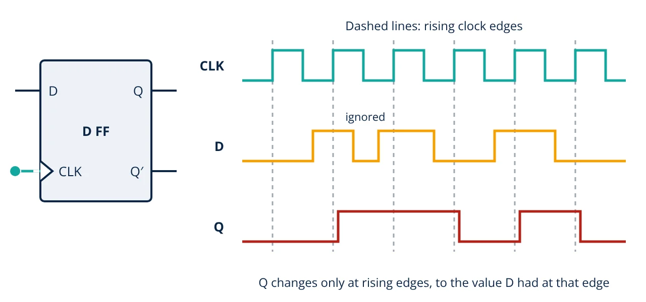
The D (data or delay) flip-flop has a single data input. At each active clock edge, Q takes the value that D has at that moment, and it holds that value until the next active edge. Because there is only one input, there is no invalid combination. The figure shows a positive-edge-triggered D flip-flop: a short low pulse on D between two edges has no effect on Q.
D flip-flops are usually supplied with asynchronous preset and clear inputs, which force Q to 1 or 0 immediately, without waiting for a clock edge. They are used to put a circuit into a known state at power up. The SN74HC74, for example, contains two positive-edge-triggered D flip-flops with active low preset and clear.
T flip-flop
The T (toggle) flip-flop has one input T. When T = 0 the output holds; when T = 1 the output toggles at every active clock edge. A T flip-flop is made by tying the J and K inputs of a JK flip-flop together, or by feeding a D flip-flop with Q XOR T. With T held at 1, the output frequency is half the clock frequency, which is why T flip-flops are the building block of binary counters and frequency dividers.
| T | Q next | Action |
|---|---|---|
| 0 | Q | No change |
| 1 | Q′ | Toggle |
Characteristic equations of flip-flops
The next state Q(n+1) after a clock edge can be written as a Boolean function of the inputs and the present state Q(n):
For designing counters and state machines, the reverse question matters: which inputs produce a required transition? This is the excitation table (X means either value works).
| Q to Q next | S R | J K | D | T |
|---|---|---|---|---|
| 0 to 0 | 0 X | 0 X | 0 | 0 |
| 0 to 1 | 1 0 | 1 X | 1 | 1 |
| 1 to 0 | 0 1 | X 1 | 0 | 1 |
| 1 to 1 | X 0 | X 0 | 1 | 0 |
Timing rules: setup, hold and propagation delay
Real flip-flops need time to respond, and datasheets specify three key parameters:
- Setup time: the minimum time the input must be stable before the active clock edge.
- Hold time: the minimum time the input must remain stable after the edge.
- Propagation delay: the time from the clock edge to the change at the output Q.
If the input changes inside the setup and hold window, the flip-flop can become metastable: its output may hover between logic levels or settle late to an unpredictable value. Signals that arrive from an unrelated clock domain, such as a push button or a serial line, are therefore passed through a synchronizer of two flip-flops in series, which gives the first stage time to settle before the second samples it. In a synchronous design the maximum clock frequency is set by the clock to output delay, the logic delay between flip-flops and the setup time.
Worked example: a ripple counter
- Given
- Four T flip-flops with T = 1 connected as an asynchronous (ripple) counter. The first is driven by a 10 MHz clock, and each later stage is clocked by the Q output of the previous one. Propagation delay of each flip-flop: 10 ns.
- Find
- (a) The output frequency of the last stage. (b) The counter modulus. (c) The worst case ripple delay and whether all outputs settle within one clock period.
- Assumptions
- Each stage toggles once per active edge of its input; the delays add because each stage waits for the one before it.
- Solution
- (a) Each stage divides by 2, so f_out = 10 MHz ÷ 2⁴ = 10 MHz ÷ 16 = 0.625 MHz
(b) Modulus = 2⁴ = 16 states, counting 0 to 15
(c) Worst case delay = 4 × 10 ns = 40 ns. Clock period = 1 ÷ 10 MHz = 100 ns. Since 40 ns is less than 100 ns, every output settles before the next clock edge. - Answer
- The last stage gives 625 kHz, the counter has 16 states, and the 40 ns ripple delay fits within the 100 ns clock period
- Limitations
- During the 40 ns ripple, the outputs briefly show wrong intermediate counts, which can cause glitches in decoding logic. Synchronous counters, where all flip-flops share one clock, avoid this.
Applications of flip-flops
- Registers: a group of D flip-flops sharing a clock stores a byte or word, as in the registers of a microprocessor.
- Shift registers: flip-flops in a chain move data one position per clock, for serial to parallel conversion.
- Counters and frequency dividers: T or JK flip-flops count pulses and divide clock frequencies.
- State machines: the present state is held in flip-flops and the next state logic is combinational, the basis of controllers and of the control unit in a processor architecture.
- Synchronizers and debouncing: flip-flops align external signals with the system clock.
Key formulas for flip-flops
| Quantity | Formula | Symbols and units |
|---|---|---|
| SR next state | Q(n+1) = S + R′Q(n), with S·R = 0 | S, R inputs; Q(n) present state |
| JK next state | Q(n+1) = JQ′(n) + K′Q(n) | J, K inputs |
| D next state | Q(n+1) = D | D data input |
| T next state | Q(n+1) = T ⊕ Q(n) | T toggle input |
| Ripple counter output | f_out = f_clk ÷ 2ⁿ | n = number of stages, f in Hz |
| Counter modulus | M = 2ⁿ | number of states |
| Ripple delay | t_total = n × t_pd | t_pd = delay per flip-flop, in ns |
Flip-flops interview and viva questions
- What is the main difference between a latch and a flip-flop? A latch is level sensitive and transparent while enabled, whereas a flip-flop is edge triggered and samples its inputs only at a clock edge.
- Why is S = R = 1 not allowed in an SR flip-flop? Both outputs are forced to the same level, so Q and Q′ are no longer complements, and the state after the inputs are removed is unpredictable.
- What is the race-around condition? In a level-triggered JK flip-flop with J = K = 1, the output can toggle many times during one long clock pulse; master-slave and edge-triggered designs prevent it.
- How do you convert a JK flip-flop into a T flip-flop? Tie J and K together and use the joined input as T, so T = 1 gives toggle and T = 0 gives hold.
- What causes metastability and how is it reduced? It occurs when the input changes within the setup and hold window around the clock edge; a two flip-flop synchronizer gives the signal time to settle before it is used.
Related reading
Frequently asked questions
What is the difference between a latch and a flip-flop?
A latch is level sensitive: while its enable input is active, the output follows the inputs. A flip-flop is edge triggered: it samples its inputs only at a clock edge and holds the result until the next active edge.
Why is the D flip-flop the most widely used type?
It has a single data input, so it cannot enter an invalid state, and its next state is simply the value of D at the clock edge. Registers, pipelines and synchronous logic in FPGAs and processors are built mainly from D flip-flops.
How does a T flip-flop divide frequency by two?
With T held at 1, the output toggles on every active clock edge. Two clock edges of the same direction are needed for one full output cycle, so the output frequency is half the clock frequency.
References
- M. M. Mano and M. D. Ciletti, Digital Design, 5th ed., Pearson
- T. L. Floyd, Digital Fundamentals, 11th ed., Pearson
- P. Horowitz and W. Hill, The Art of Electronics, 3rd ed., Cambridge University Press
- Texas Instruments, SN74HC74 Dual D-Type Positive-Edge-Triggered Flip-Flops With Clear and Preset, datasheet
- IEEE Std 91-1984, IEEE Standard Graphic Symbols for Logic Functions
Get one engineering email a week
New articles, worked examples and study notes every week. Free, no spam, unsubscribe any time.

Electronics and Telecommunication engineer working in industrial instrumentation and automation. Writes the Electronics Engineering articles on Zenta Engineering. Editorial policy.