Boost Converter Working Principle and Design
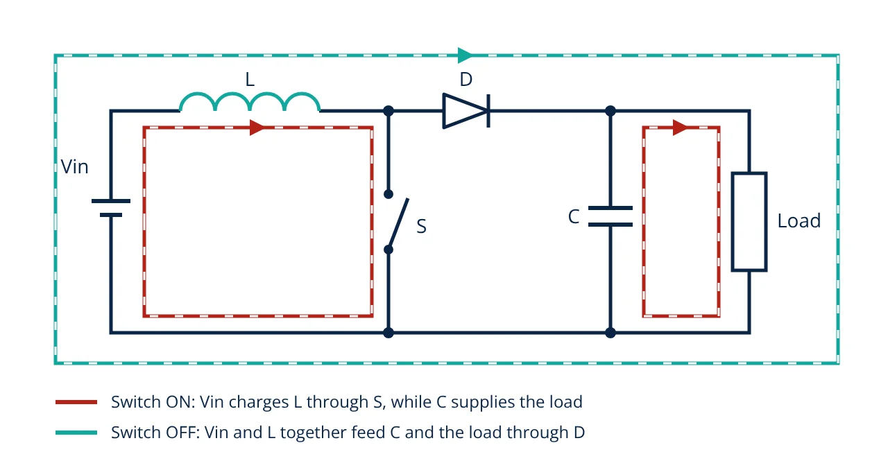
A boost converter is a switching DC-DC converter that steps a DC voltage up. A transistor switch first stores energy in an inductor, then releases it through a diode to the output capacitor and load. In continuous conduction the ideal output voltage is Vout = Vin / (1 − D), where D is the duty cycle.
A boost converter raises a low DC voltage, such as a single lithium cell or a 5 V USB rail, to a higher regulated voltage. It uses the same four parts as a buck converter, arranged differently, and it relies on the fact that an inductor resists any sudden change in its current. This article explains the working principle, the design equations, component selection and a complete design example.
Boost converter circuit and components
The boost converter has four power components:
- Switch S, usually an n-channel MOSFET from the switch node to ground, turned on and off by a pulse width modulation (PWM) controller. Its operation is covered in transistor working principle.
- Inductor L, in series with the input. It stores energy when the switch is on and keeps the input current flowing when the switch is off.
- Diode D, usually a Schottky diode, which passes current to the output only when the switch is off and blocks the output capacitor from discharging through the switch.
- Output capacitor C, which holds the output voltage up and supplies the load while the diode is not conducting.
How a boost converter works step by step
- Switch on (time D × T). The switch connects the right end of the inductor to ground. The full input voltage appears across L, so the inductor current rises linearly and energy builds up in its magnetic field. The diode is reverse biased because its cathode is at Vout, and the capacitor alone supplies the load.
- Switch off (time (1 − D) × T). The inductor current cannot change instantly, so the switch node voltage rises until the diode conducts. The inductor now has Vin − Vout across it, which is negative, and its current falls linearly. The source and the inductor act in series, so the output receives a voltage higher than the input.
- Repeat. The controller repeats this at the switching frequency fsw and adjusts D to hold the output at its set value as the input voltage and load change.
In steady state the inductor current must return to the same value at the end of every period, so the average inductor voltage is zero (volt-second balance):
Because an ideal converter has no losses, input power equals output power. The average input current, which is also the average inductor current, is therefore larger than the output current:
Boost converter design equations
Duty cycle. Rearranging the gain equation gives D = 1 − Vin / Vout. Use the minimum input voltage when sizing the inductor and switch, because that is where D and the input current are largest.
Inductor ripple current. During the on time the full input voltage is across the inductor, so:
Texas Instruments SLVA372 suggests a starting estimate of 20 to 40 percent of the output current, scaled by Vout / Vin, for the ripple current.
Peak switch and inductor current. IL(peak) = Iin + ΔIL / 2. The inductor saturation rating and the switch current limit must both exceed this value with margin.
Output voltage ripple. While the switch is on, the capacitor alone carries the full load current for the time D × T, so:
The capacitor’s ESR adds further ripple, because the capacitor sees the pulsed diode current. Low ESR ceramic capacitors are the usual choice.
Voltage stress. The switch and the diode both see about Vout when they are off, so each needs a voltage rating above the maximum output voltage. The average diode current equals the output current.
Key formulas for boost converter design
| Quantity | Formula | Symbols and units |
|---|---|---|
| Ideal output voltage | Vout = Vin / (1 − D) | V; D = duty cycle, 0 to 1 |
| Duty cycle | D = 1 − Vin / Vout | dimensionless |
| Average input current | Iin = Iout / (1 − D) | A; equals average inductor current |
| Inductor ripple | ΔIL = Vin × D / (L × fsw) | A; L in H, fsw in Hz |
| Peak inductor current | IL(peak) = Iin + ΔIL / 2 | A |
| Output ripple | ΔVout = Iout × D / (fsw × C) | V; C in F, ESR ignored |
- Given
- Vin = 5 V, Vout = 12 V, Iout = 0.5 A, fsw = 500 kHz, inductor ripple target 30 percent of Iout × Vout / Vin, output ripple target 50 mV.
- Find
- Duty cycle, inductor value, average and peak inductor current, and output capacitance.
- Assumptions
- Ideal components, continuous conduction, capacitor ESR ignored for the first estimate.
- Solution
- D = 1 − 5 / 12 = 0.583
ΔIL target = 0.3 × 0.5 × 12 / 5 = 0.36 A
L = 5 × 0.583 / (500,000 × 0.36) = 16.2 µH, so choose 22 µH
Actual ΔIL = 5 × 0.583 / (500,000 × 0.000022) = 0.265 A
Iin = 0.5 / (1 − 0.583) = 1.2 A
IL(peak) = 1.2 + 0.265 / 2 = 1.33 A
C = 0.5 × 0.583 / (500,000 × 0.05) = 11.7 µF, so choose 22 µF ceramic, giving about 26.5 mV of ripple - Answer
- D ≈ 0.58, L = 22 µH rated above 1.33 A with margin, C = 22 µF low ESR ceramic, switch and diode rated above 12 V
- Limitations
- Losses raise the real duty cycle and the input current. Ceramic capacitors lose capacitance under DC bias, so check the effective value at 12 V. The control loop must be compensated for the right half plane zero.
Losses and practical limits
The main losses are the same as in other switching converters:
- Switch conduction loss: the RMS switch current squared times RDS(on).
- Switching loss: energy lost in each turn-on and turn-off, rising with switching frequency and output voltage.
- Diode loss: forward voltage times the output current, plus reverse recovery loss in non-Schottky diodes. A synchronous boost replaces the diode with a MOSFET to reduce this.
- Inductor loss: winding resistance and core loss. The inductor carries the full input current, which is larger than the output current.
- Capacitor loss: ripple current through ESR.
Erickson and Maksimović show that the inductor winding resistance limits the voltage gain. With losses, the real gain reaches a maximum and then falls as D approaches 1, so the ideal equation is only valid at moderate duty cycles.
A boost converter also has no way to disconnect the load. When the switch is off, the input connects to the output through L and D, so the output cannot fall below Vin minus a diode drop, and a short circuit on the output is not limited by the switch. Startup inrush into the output capacitor is a related issue. Many integrated boost regulators add a load disconnect switch for this reason.
Continuous and discontinuous conduction
In continuous conduction mode (CCM), the inductor current never reaches zero and Vout = Vin / (1 − D). At light load the inductor current falls to zero before the end of each period. In this discontinuous conduction mode (DCM), the gain depends on the load as well as D, and the controller must adjust D further. Many controllers use pulse skipping at light load to keep efficiency high.
Control and the right half plane zero
Mohan and Erickson both show that the CCM boost converter has a right half plane zero in its control-to-output transfer function. When D increases, the diode conducts for a shorter part of each period, so the output dips for a moment before the larger inductor current raises it. This limits the crossover frequency of the voltage loop, and current mode control is common in practice.
Boost converter applications
- Battery powered devices that raise a single cell voltage to 5 V or higher rails.
- LED backlight and string drivers, where many LEDs in series need more voltage than the supply.
- Power factor correction front ends. Mohan describes the boost converter as the usual PFC stage, because its input inductor gives a continuous input current that can be shaped to follow the line voltage. This helps equipment meet the harmonic current limits of IEC 61000-3-2 and improves power factor. A practical description of this circuit is in this boost PFC circuit explanation.
- Solar and fuel cell systems, where a low, varying source voltage must be raised to a DC bus.
Layout matters as much as component choice. In a boost converter the fast switching loop is the output loop formed by the switch, the diode and the output capacitor, so keep it as small as possible, as described in PCB design basics.
Boost converter interview and viva questions
- What is the ideal voltage gain of a boost converter? In continuous conduction it is Vout / Vin = 1 / (1 − D), derived from volt-second balance on the inductor.
- Why is the input current of a boost converter larger than the output current? Power in equals power out in an ideal converter, and the output voltage is higher, so the average input current is Iout / (1 − D).
- What voltage rating do the switch and diode need? Each sees about the output voltage when it is off, so both are rated above the maximum output voltage with margin.
- What is the right half plane zero? It is a zero in the control-to-output transfer function of a CCM boost converter that makes the output first move the wrong way after a duty cycle increase, which limits loop bandwidth.
- Why can a basic boost converter not protect against an output short circuit? The input is connected to the output through the inductor and diode whenever the switch is off, so turning the switch off cannot interrupt the fault current.
Related reading
Frequently asked questions
Can a boost converter produce an output lower than its input?
No. When the switch is off there is a direct path from the input through the inductor and diode to the output, so the output sits at about the input voltage minus one diode drop even with the switch idle. A buck-boost or SEPIC topology is needed when the output must go below the input.
Why does a boost converter need a high duty cycle for large voltage gain?
The ideal gain is 1 / (1 − D), so the gain only becomes large as D approaches 1. In a real converter the resistance of the inductor, switch and diode makes the gain reach a maximum and then fall at very high duty cycle, so large step-up ratios are usually done with transformer-isolated or cascaded converters instead.
Why is a boost converter harder to control than a buck converter?
In continuous conduction the boost converter has a right half plane zero in its control-to-output transfer function. Increasing D first shortens the time the diode delivers current, so the output briefly moves the wrong way before it rises. This limits the usable loop bandwidth of the voltage control loop.
References
- R. W. Erickson and D. Maksimović, Fundamentals of Power Electronics, 3rd ed., Springer, 2020
- N. Mohan, T. M. Undeland and W. P. Robbins, Power Electronics: Converters, Applications, and Design, 3rd ed., Wiley, 2003
- M. H. Rashid, Power Electronics: Devices, Circuits, and Applications, 4th ed., Pearson, 2014
- Texas Instruments, SLVA372, Basic Calculation of a Boost Converter's Power Stage, application report
- IEC 61000-3-2:2018 Electromagnetic compatibility (EMC), Part 3-2: Limits, Limits for harmonic current emissions (equipment input current up to and including 16 A per phase)
Get one engineering email a week
New articles, worked examples and study notes every week. Free, no spam, unsubscribe any time.

Electronics and Telecommunication engineer working in industrial instrumentation and automation. Writes the Electronics Engineering articles on Zenta Engineering. Editorial policy.